
Dr. Wiston Schoenfeld
Dr. Winston Schoenfeld is a chemistry professor here at UCF who works in the chemistry department at the CREOL laboratory of optic and photonics. One of Dr. Schoenfeld areas of research deals with the growth of materials specially semiconductors, that would be used for applications such as the detection or generation of light ort in other words emitters or detectors.
A new type of semiconductors or especially known as the oxide semiconductors that have really never been studied before; until now. This new type of semiconductor could offer a platform to create detectors or light emitters in an light spectrum of interest in this case the solar blind region.
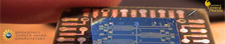
Dr. Schoenfeld ‘s research group has been able to pioneer the re-systemization of films that in fact are oxide semiconductors. By doing this his research group is able to study the properties of these oxide semiconductors. Some of the semiconductors that his team is currently working with are nickel magnesium oxide among others similar materials. When Studying and classifying the properties of these materials the researchers group is able to choose either to synthesize materials with high qualities characteristics in the solar blind optical region. By doing this the transmitters can emit or detect. I addition, for making the highest quality materials possible, the device quality performance is directly related to the materials the device is made of. Also, Dr. Schoenfeld research group must design the devices themselves in order to study the qualities of layers in a structure. For example a layer of a structure might be synthesized in order so that when it becomes exposed to a current it would to produce light or when it becomes exposed to a light pattern this would produce a current in order to identify the presence of a certain light pattern. Up to date, Dr. Schoenfeld research group has been able to show that both nickel and by using the Molecular Bean Epitaxy (MBE System). An MBE is a high vacuum chamber and controlled environment in which a substrate in this case magnesium oxide is inserted into. Inside the MBE the substrate will be beamed with source materials. For example nickel magnesium oxide were to be created in the MBE it would have to be made from a sort of sources that would heat up like an oven, therefore emitting atoms towards the surface of the sample that is being synthesized, also a magnesium source fed into the sample. In addition to this there will be an oxygen source which will also release atoms in order to make a nickel magnesium oxide film. The size of one of these films could anywhere from one centimeter square up to three to four inches in diameter this films are significantly thin they cold be one micron thin; however this is thick enough in order to create a light detector.

Molecular Bean Epitaxy (MBE System)
Some of these semiconductors thin films is their ability to store memory, meaning theses could be used in future computer components. In addition, these semiconductors are able to detect low magnetic fields giving us more accurate readings in the presence of magnetic fields. Also, in the future these semiconductors in the form of light emitters that will produce light that will have a have a wave length of less than 280 nm in order to literally destroy any form of bacteria including RNA and DNA. These semiconductors could be also be used in the form of detectors in the military area in order to detect bio hazard agents and other things such as missile plume since these semiconductors are not disrupted from the background sound produce by the sun.